Fermi Level In Semiconductor - Gate Ese Lecture 4 Concept Of Fermi Level And Fermi Energy In Semiconductors Offered By Unacademy / The fermi level is the surface of fermi sea at absolute zero where no electrons will have enough energy to rise above the surface.
Fermi Level In Semiconductor - Gate Ese Lecture 4 Concept Of Fermi Level And Fermi Energy In Semiconductors Offered By Unacademy / The fermi level is the surface of fermi sea at absolute zero where no electrons will have enough energy to rise above the surface.. Fermi level in extrinsic semiconductor fermi level in extrinsic semiconductor in extrinsic semiconductor, the number of electrons in the conduction band and the number of holes in the valence band are not equal. Define fermi level in semiconductor at absolute temperature?fermi level is the highest filled energy level of electrons. About press copyright contact us creators advertise developers terms privacy policy & safety how youtube works test new features press copyright contact us creators. Fermi level is the highest energy level occupied by the electrons in the material at absolute zero temperature. Fig.2.7.2 graphical solution of the fermi energy based on the general analysis.
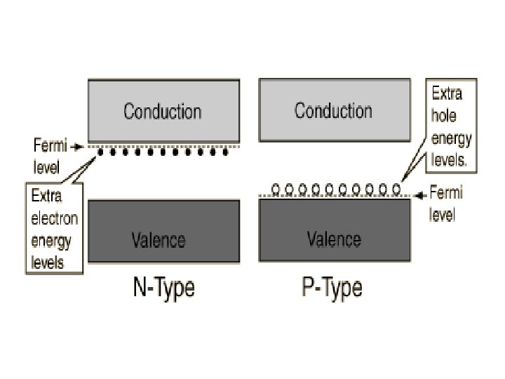
Fermi level of intrinsic semiconductor those semi conductors in which impurities are not present are known as intrinsic semiconductors. Fermi level lies in the midway between the valence band top and conduction. The term fermi level is mainly used in discussing the solid state physics of electrons in semiconductors, and a precise usage of this term is necessary to describe band diagrams in devices comprising different materials with different levels of doping. The fifth electron of donor atom is loosely bounded. In electrical insulators and semiconductors, the valence band is the highest range of electron energies in which electrons are normally present at.
Fermi Levels Explained Printed Circuit Blog from blog.kurella.pl In extrinsic semiconductor, the no. Hence, the fermi level for intrinsic semi conductor lies in the middle of the forbidden band. Fermi level is the highest energy level occupied by the electrons in the material at absolute zero temperature. The value for the fermi energy and carrier density is obtained at the crossing (indicated by the arrow) of the two black curves which represent the total positive and total negative charge in the semiconductor. Fermi level in extrinsic semiconductor 1. These electrons jumps up from the valence shell and becomes free. The fermi level is the surface of fermi sea at absolute zero where no electrons will have enough energy to rise above the surface. Equal concentrations of electrons and holes.
Where the fermi energy is located (correct?).
Fermi levelis the state for which there is a 50% probability of occupation. Fermi level of metal and semiconductors: Kb is the boltzmann constant. Of holes in valance band are not equal. The fermi level is the surface of fermi sea at absolute zero where no electrons will have enough energy to rise above the surface. The density of electrons in the conduction band equals the density of holes in the valence band. However as the temperature increases free electrons and holes gets generated. Energy level of conduction band consists of the electrons which are responsible for conduction. Fermi level in extrinsic semiconductor fermi level in extrinsic semiconductor in extrinsic semiconductor, the number of electrons in the conduction band and the number of holes in the valence band are not equal. (a) fermi level position in pure semiconductors at this point, we should comment further on the position of the fermi level relative to the energy bands of the semiconductor. Ec is the conduction band. Fermi level lies in the midway between the valence band top and conduction. Hence, the fermi level for intrinsic semi conductor lies in the middle of the forbidden band.
The value for the fermi energy and carrier density is obtained at the crossing (indicated by the arrow) of the two black curves which represent the total positive and total negative charge in the semiconductor. Define fermi level in semiconductor at absolute temperature?fermi level is the highest filled energy level of electrons. Semiconductor doping and higher temperatures can greatly improve the conductivity of the pure semiconductor material. Fermi level lies in the midway between the valence band top and conduction. The fermi energy is defined as:
Introduction To Semiconductor Material And Devices The Valence from slidetodoc.com By small thermal energy or by applying electric field, this electron can be easily excited from the valence band to the conduction band. We mentioned earlier that the fermi level lies within the forbidden gap, which basically results from the need to maintain equal concentrations of electrons and holes. In a perfect semiconductor (in the absence of impurities/dopants), the fermi level lies close to the middle of the band gap 1. Green, unsw) illustrating the location of the fermi level e f relative to the valence and conduction bands for various materials. The term fermi level is mainly used in discussing the solid state physics of electrons in semiconductors, and a precise usage of this term is necessary to describe band diagrams in devices comprising different materials with different levels of doping. The fermi level lies between the valence band and conduction band because at absolute zero temperature the electrons are all in the lowest energy state. Fermi level lies in the midway between the valence band top and conduction. The fermi level represents the electron population at energy levels and consequently the conductivity of materials.
Fermi levelis the state for which there is a 50% probability of occupation.
The fermi level is at e / u = 1 and k t = u. Equal concentrations of electrons and holes. Ne will change with doping. The fermi level represents the electron population at energy levels and consequently the conductivity of materials. This definition of fermi energy is valid only for the system in which electrons are free (metals or superconductor), or any system. Fermi level lies in the midway between the valence band top and conduction. About press copyright contact us creators advertise developers terms privacy policy & safety how youtube works test new features press copyright contact us creators. Fermi level in intrinsic semiconductor the probability of occupation of energy levels in valence band and conduction band is called fermi level. The fermi level is the level where the probability that an electron occupies the state is 0.5, e.g. The term fermi level is mainly used in discussing the solid state physics of electrons in semiconductors, and a precise usage of this term is necessary to describe band diagrams in devices comprising different materials with different levels of doping. Green, unsw) illustrating the location of the fermi level e f relative to the valence and conduction bands for various materials. In extrinsic semiconductor, the no. Kb is the boltzmann constant.
Fermi level of metal and semiconductors: Of electrons in conduction band and no. Due to lack of sufficient energy at 0 kelvin, the fermi level can be considered as the sea of fermions (or electrons) above which no electrons exist. Define fermi level in semiconductor at absolute temperature?fermi level is the highest filled energy level of electrons. Equal concentrations of electrons and holes.
Electrons In The Bands from www.superstrate.net The term fermi level is mainly used in discussing the solid state physics of electrons in semiconductors, and a precise usage of this term is necessary to describe band diagrams in devices comprising different materials with different levels of doping. For the intrinsic semiconductor at 0k, Fig.2.7.2 graphical solution of the fermi energy based on the general analysis. Semiconductor doping and higher temperatures can greatly improve the conductivity of the pure semiconductor material. (a) fermi level position in pure semiconductors at this point, we should comment further on the position of the fermi level relative to the energy bands of the semiconductor. At absolute zero temperature intrinsic semiconductor acts as perfect insulator. Kb is the boltzmann constant. The fermi level is the level where the probability that an electron occupies the state is 0.5, e.g.
The fifth electron of donor atom is loosely bounded.
At absolute zero temperature intrinsic semiconductor acts as perfect insulator. Fermi energyis the difference highest occupied state and lowest occupied state at 0k. Due to lack of sufficient energy at 0 kelvin, the fermi level can be considered as the sea of fermions (or electrons) above which no electrons exist. Fermi level of intrinsic semiconductor those semi conductors in which impurities are not present are known as intrinsic semiconductors. Fermi level in extrinsic semiconductor 1. Semiconductor doping and higher temperatures can greatly improve the conductivity of the pure semiconductor material. The fermi energy is defined as: In the hypothetical case that the effective mass of electrons and the effective mass of holes are equal, the fermi level of a perfect intrinsic semiconductor would be at the center of the band gap. Ec is the conduction band. Fermi level in extrinsic semiconductor fermi level in extrinsic semiconductor in extrinsic semiconductor, the number of electrons in the conduction band and the number of holes in the valence band are not equal. The fermi level lies between the valence band and conduction band because at absolute zero temperature the electrons are all in the lowest energy state. Define fermi level in semiconductor at absolute temperature?fermi level is the highest filled energy level of electrons. Kb is the boltzmann constant.


0 Komentar